Site card
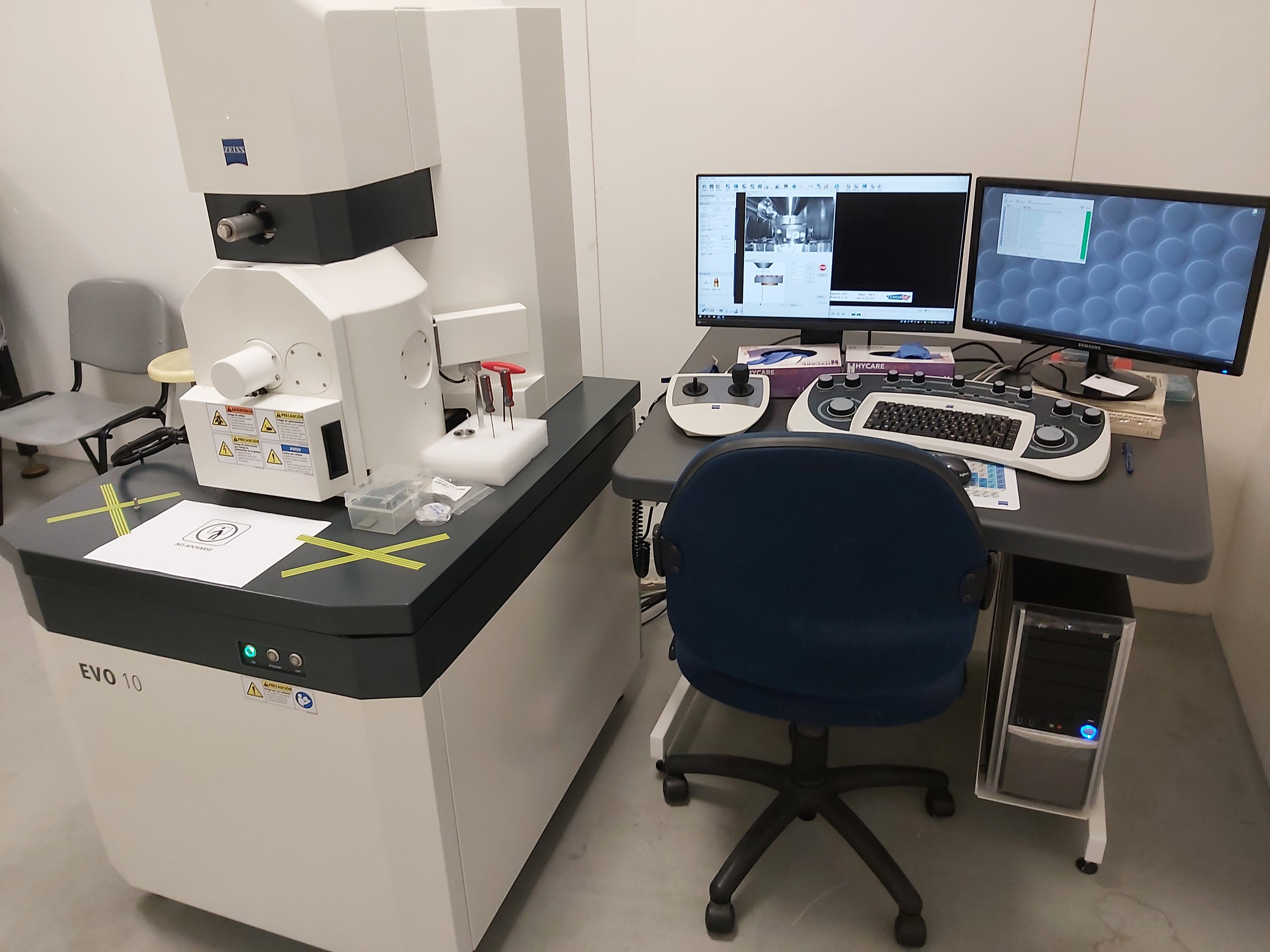
Zeiss EVO 10 SEM
Where:
Centre of Advanced Materials and Devices for Information and Communications Technology (CEMDATIC)
Ubicación:
ETSI de Telecmunicación, A409L
Typology:
Equipamiento científico-Tecnológico
Manager: Teona Mirea
Email:
EVO10 automated, high-resolution scanning electron microscope, including secondary electron detector, control PC, joystick and control panel.
Microtechnology, Nanotechnology, Microelectronics, Photonics
Microscopes of this type provide images of the surfaces of various samples, with resolutions of a few nanometres (nm). They are based on the interaction of electrons with the sample material. Their small size makes it possible to open, close and empty the chamber in 1 to 2 minutes, opening up the possibility of analysing many more samples in a shorter amount of time. Their working resolution can reach 1 to 3 nm, depending on the material to be analysed.
- Analysis of 3D microstructures with angled images. These structures will be printed to produce free-form lenses, mirrors and other novel designs. - Analysis of functional layers to be integrated into both gas and biological electro-acoustic microsensors. The thickness of such layers ranges between 5 and 50 nm. - Analysis of carbon nanotubes with diameters ranging from 1 to several nanometres. - Decoration of different microstructures with nanoparticles for use in microsensors. - For the manufacture of microsensors and high-pass filters.
- 3D microstructures for producing free-form lenses, mirrors and other novel designs. Two-photon polymerisation makes it possible to print optically transparent microstructures with smooth surfaces throughout a thin process. The technology is not only used to manufacture microparts on flat substrates, but also to print complex structures directly and precisely onto pre-existing patterns and topographies, such as photonic integrated circuits, optical fibre tips and prefabricated wafers. This method makes it possible to miniaturise optical interfaces and manufacture them without assembly, using in situ high-precision 3D microprinting in various materials, such as InP, SOI and Si3N4. - Nanofiltration and detection of nanoparticles using carbon nanotubes integrated into electro-acoustic sensors. - Manufacture of micro-resonators for sensors and high-pass filters.


