Site card
Metalorganic vapour-phase epitaxy (MOVPE) reactor
Where:
III-V semiconductors
Ubicación:
Planta baja Instituto de Energía Solar
Typology:
Infraestructura Científica
Manager: Prof. Carlos Algora
Email:
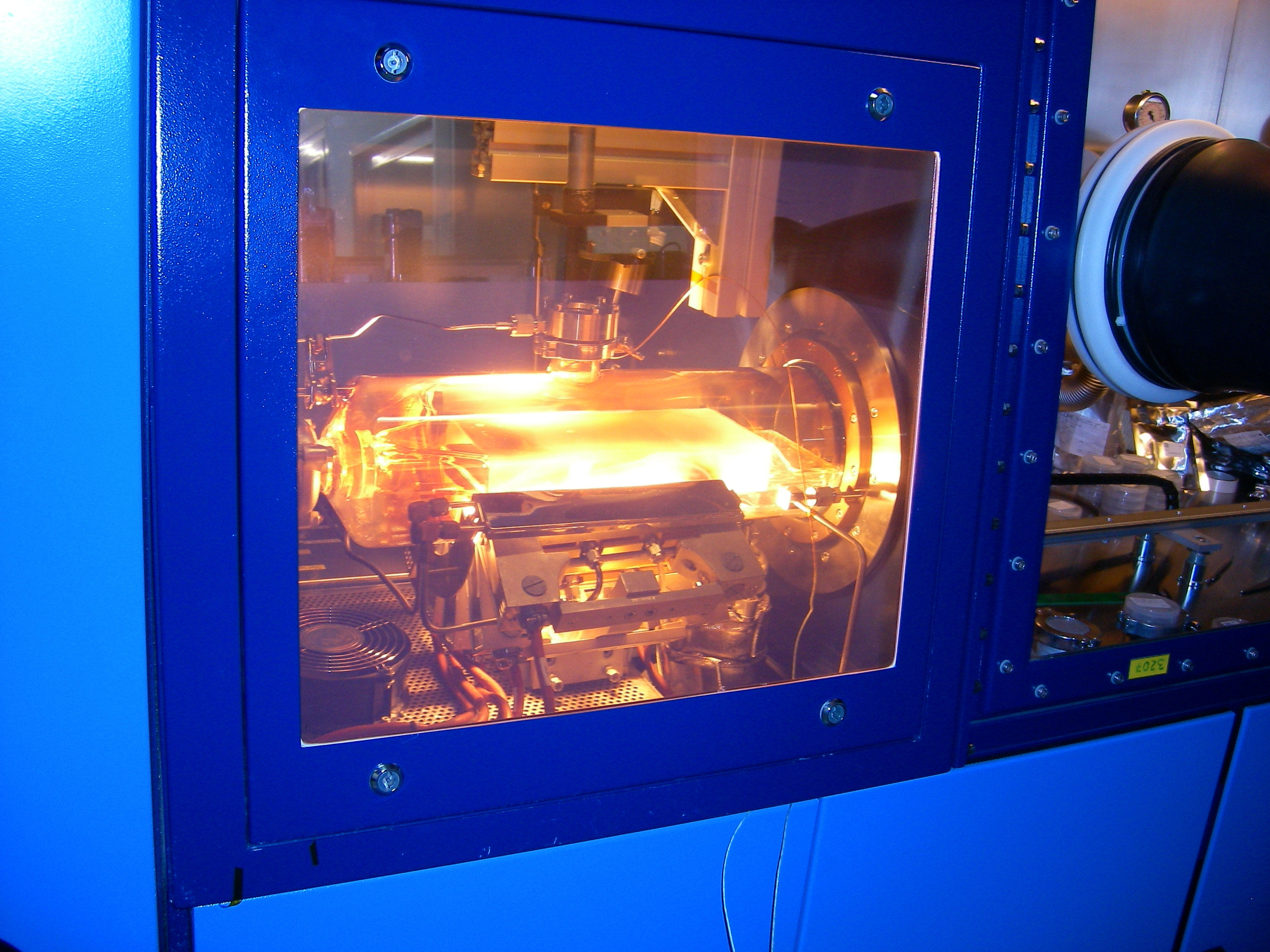
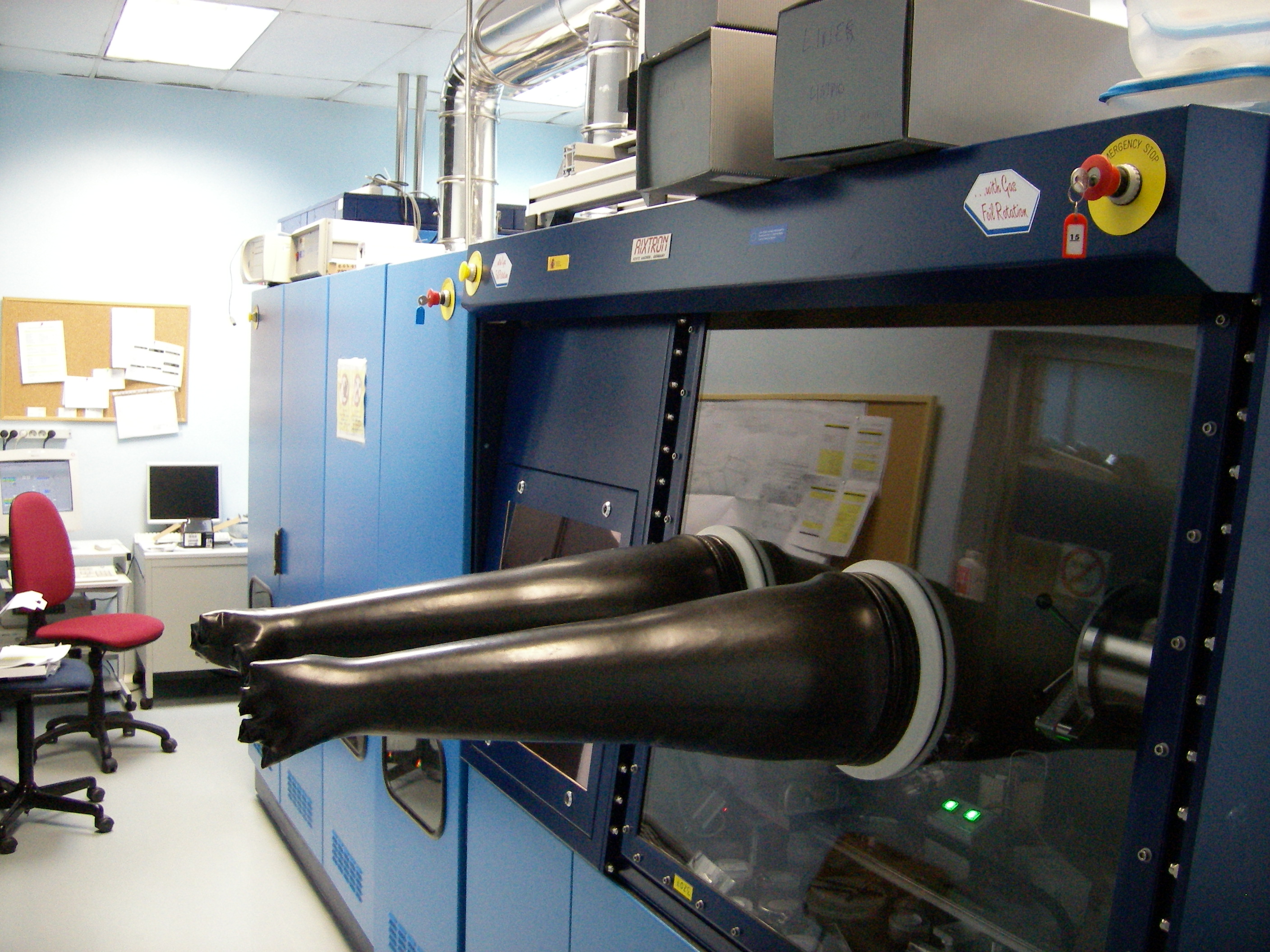
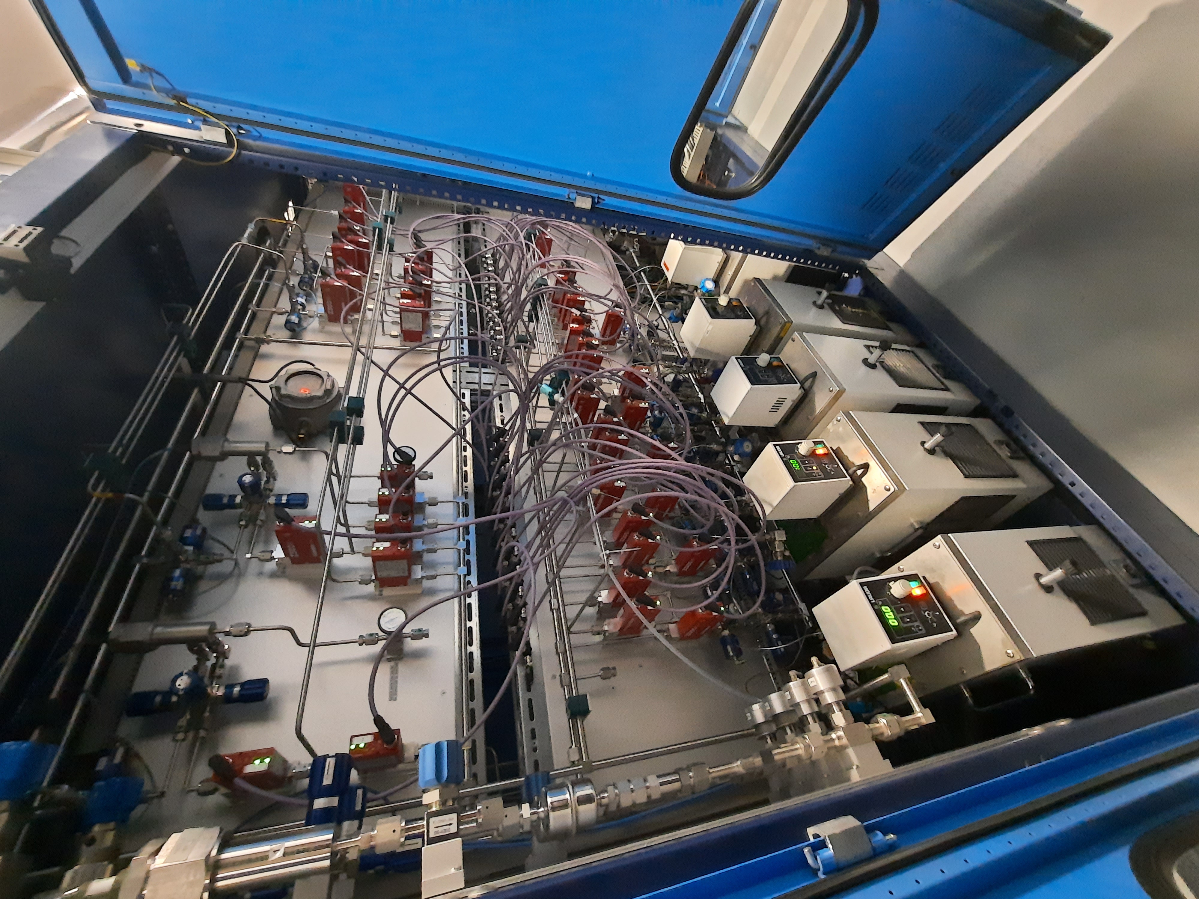
The MOVPE reactor is the AIXTRON AIX/200-4 model. It measures 6 metres (length) x 1.4 metres (width) x 2.4 metres (height) and weighs approximately 3200 kg.
- Photovoltaic solar energy (solar cells) - Optoelectronics (lasers, LEDs, photodiodes, etc.)
It makes it possible to grow dozens of layers of III-V semiconductors, including GaAs, InP, GaP, InGaAs, AlGaAs, GaInP, AlInP and diluted nitrides of these families, among others, with thicknesses varying from nanometres to several microns and a very wide doping range. The layers can be grown on semiconductor substrates such as GaAs, Si, Ge and InP, with sizes of 2, 3 and 4 inches. Devices are subsequently manufactured on the semiconductor structure grown.
It is currently used to grow semiconductor structures to manufacture solar cells for land and space applications (including flexible cells), laser light converters and thermophotovoltaic devices.
It can be used to grow semiconductor structures that give rise to devices with disruptive applications in optoelectronics. It also allows semiconductor layers to be grown on substrates including graphene.
It is the only commercial MOVPE reactor with production capacity (up to three 2-inch wafers or one 3- or 4-inch wafer) in Spain. The MOVPE reactor was completely renovated in 2021 with the help of scientific equipment grant EQC2019-005701-P from the National Research Agency (Agencia Estatal de Investigación), ERDF funds and the Universidad Politécnica de Madrid¿s own programme for co-financing R&I infrastructure.


