Site card
Laser Micro- and Nano-manufacturing Laboratory
Where:
Laser Centre
Ubicación:
90A.00.016.1; 90A.00.104.0; 90A.00.104.1; 90A.00.094.1, Centro Láser
Typology:
Infraestructura Científica
Manager: Carlos Molpeceres
Email:
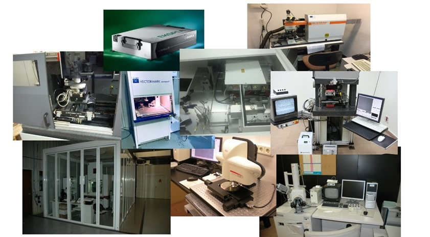
The Laser Micro- and Nano-manufacturing Laboratory has all the equipment needed to study, parameterise and perform laser processes with dimensional tolerances in the micrometric and sub-micrometric range, on any type of material. The service currently has femtosecond (fs) pulsed laser sources with a pulse width programmable to 1030 nm (EKSPLA Femtolux 30), picosecond (ps) pulsed sources at 355 nm, 532 nm and 1064 nm (LUMERA Super Rapid and Spectra Physics Vanguard), and various nanosecond (ns) sources at 355 nm, 532 nm and 1064 nm (including a high-power UV source). All of the lasers are integrated into machines or process benches and have scanners, beam control and shaping systems and different focusing systems, making it possible to use any strategy for irradiating the material and simulate process conditions in production environments. The service also has the instrumentation necessary to characterise processes in situ, including a Hitachi 3000N scanning electron microscope, a Leica DCM 3D confocal and interferometric microscope and a Raman Renishaw inVia microscope.
Laser processing, laser technology, micro-manufacturing, nano-manufacturing, advanced manufacturing, thin film processing, surface functionalisation.
Pulsed lasers with pulse widths between fs and ns are ideal tools for processing materials with micrometric and sub-micrometric resolutions. Short interaction time control, material-appropriate wavelength selection and an appropriate beam manipulation and control strategy make it possible to minimise the thermal load used in removing the material, such that those extreme tolerances are achieved in manufacturing. In addition, the infrastructure available on-site for process characterisation (SEM, confocal microscope, Raman, etc.) give the service added value, as it is possible to carry out a detailed study, using different techniques, of the state of the material after processing. Moreover, the UPM¿s Laser Centre not only has more than 20 years¿ experience in the development of processes of this kind, it is also a specialist in scaling processes to incorporate them into production lines, if required.
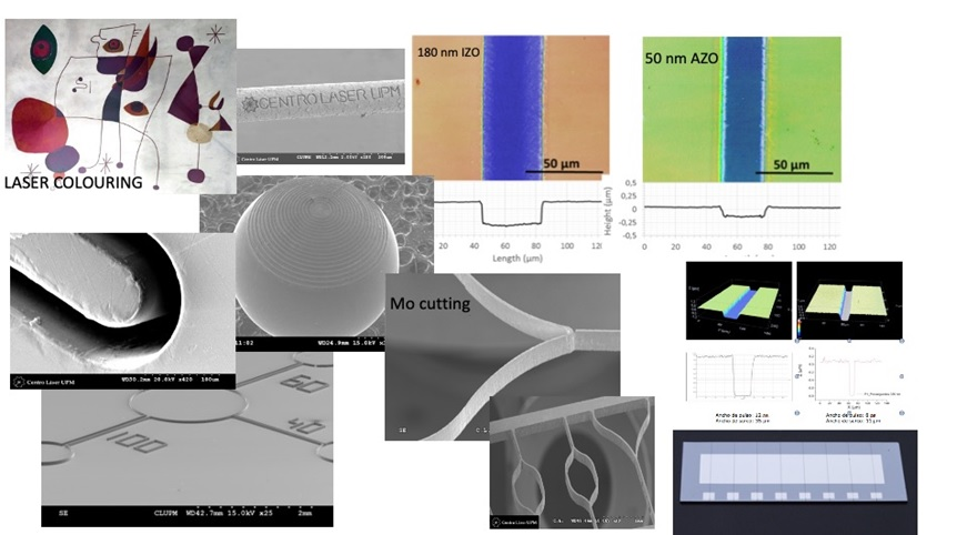
Currently, with the available infrastructure it is possible to process and characterise all kinds of materials. Some examples of the processes commonly carried out include the processing of thin films for applications in photovoltaics and electronics (insulation, interconnection, selective ablation, structuring); surface functionalisation (hierarchical structures to control wettability; control of surface roughness for biomedical applications); cutting materials to create masks for microscopy and photolithography; manufacturing channels for microfluidic devices using laser ablation; laser cleavage of silicon; laser surface modification to control optical properties; and the generation of nanometric laser-induced period structures to control light.
Laser micro- and nano-manufacturing processes are essential in the development of new technologies and devices in any strategic industrial field, from energy to biomedicine and including the automotive industry, the aerospace industry and the textile industry. Moreover, these techniques fit in perfectly with the philosophy and production methodologies of digitalised industrial environments (Industry 4.0), so significant growth in the use of this technology is expected in the coming years.
The UPM¿s Laser Centre has been a reference point, even at the international level, in the development of laser micro- and nano-manufacturing processes. Of particular note has been its contribution to the development of processes for the photovoltaic and flexible electronics industries. Moreover, belonging to the Appolo HUB network of European laboratories (www.appolohub.eu) gives it a unique view and experience of the development of this technology internationally. The Hub, created after the FP7 Appolo project, acts as a validation structure for laser processes based on pulsed lasers, helping to cover the whole value chain of European laser technology, including manufactures, equipment suppliers and industrial end users.


